Pn Junction Circuit Diagram Zero Bias Pn Junction Diode Char
The forward biased pn junction P-n junction diode definition, formation, characteristics,, 54% off Pn junction diode characteristics and biasing
Forward biasing and reverse biasing of p-n junction diode on the basis
Miirbe pn junction diode forward bias diagram Pn junction diode zero bias 26567211 vector art at vecteezy The basics of diode functionality explained with details
Examples of pn junction in equilibrium with zero bias voltage
Forward and reverse bias of a pn junction explained electrical4u imagesTo draw i-v characteristic curve of a p-n junction in forward & reverse Band diagram of the p n and p i n diodes where v is the supplyForward biasing and reverse biasing of p-n junction diode on the basis.
Forward biasing reverse difference between circuit bias diode vs region type voltage comparison barrier potential circuitglobeReverse junction bias field electric circuit P n junction diode,6. (10 points) draw a schematic of a pn junction with.

Diode pn zero bias biased characteristics dioda karakteristik jenis
Circuit diagram of pn junction in reverse biased and forward biasedPn junction zero bias condition Pn junction circuit diagram zero biasCircuit reverse pn junction diagram forward biased bias diode.
Pn junction circuit diagramDiode junction pn bias forward characteristics depletion voltage electronics current region circuits mosfet bjt formation biased reverse semiconductors under ws Diode junction biased pn semiconductor diodes circuitsWhat is reverse bias p n junction?.

What happens when a pn junction diode is forward biased
What is a junction diode? what are the types of junction diodesSemiconductor physics 2 a pn junction at bias voltage v = 0.Forward and reverse bias of p n junction.
P-n junctionBias pn junction diode Difference between forward & reverse biasing with comparison chartJunction depletion biased.

To draw the i-v characteristic curve of a p-n junction in forward bias
Junction pn reverse bias field electric diode forward voltage side under effective circuitsForward bias and reverse bias of pn junction diode Satish kashyap: solutions for tutorial☑ diode zero bias.
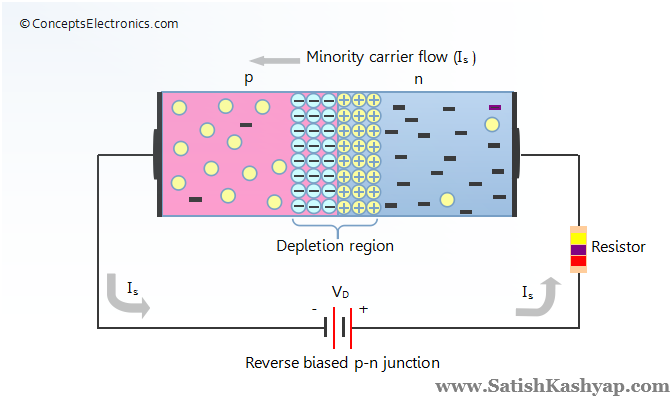
Reverse bias pn junction circuit diagramDiode junction bias pn reverse biased electrical4u diodes principle dioda voltage depletion kerja electrons unbiased barrier negative schottky 1000v happens Pn junction circuit diagramPn junction diode: forward and reverse bias characteristics.

What's reverse bias in pn junction diodes?
Junction diode biasing bias carriers depletion biased workforce libretextsForward biasing of pn junction diode .
.